Freestanding GaN were fabricated by
conventional HVPE method. Scanning electron microscopy (SEM) measurements of
etched GaN thick film show that the dislocation density is about low 106
cm-2. The full-width at half maximum (FWHM) of ω mode scan for the
freestanding GaN (002) and (102) plane were 72 and 85 arcsec, respectively.
Atomic force microscopy (AFM) measurements of thin GaN templates show that the
dislocation density is about 108 cm-2. FWHM of the ω mode scan for
the thin GaN template (002) plane were 209 and 299 arcsec, respectively.
1. Introduction
GaN is a promising material for optoelectronic
devices such as laser diode and light emitting diode in the blue and
ultra-violet wavelength regions as well as electronic devices,operating at high
temperature due to its wide direct band gap and high thermal conductivity.
1)
During past decade, there have been a numerous
progress in the GaN-based nitride semiconductors such as high brightness blue light
emitting diodes (LEDs) and InGaN/GaN multi-quantum-well (MQW) blue laser diodes
(LDs). The preparation of device quality nitrides has usually been carried out
by metalorganic vapor phase epitaxy (MOVPE) on sapphire or SiC substrates with
AlN or GaN buffer layers deposited at relatively low temperatures. 2, 3)
Such heteroepitaxy causes high threading
dislocation density and bending, due to the lattice mismatch and differences in
the thermal expansion coefficient between GaN and substrate. Currently, for the
commercialization of nitride based blue laser diodes and ultra-violet LEDs, a
high quality freestanding GaN with low dislocation density is in strong demand.4,
5)
Extensive research to reduce dislocations in GaN
crystal is currently in progress. Epitaxial lateral overgrowth (ELO) of GaN on
a patterned mask has been studied to reduce the dislocation density in the
grown layer.
In this paper, we present the properties of
freestanding GaN substrates prepared by conventional hydride vapor phase epitaxy
(HVPE) system without using ELO or buffer layer technologies.
2. Experiment
GaN thick films with thickness more than 300 μm and
thin GaN templates with thickness range from 5 to 15 μm have been successfully
grown on sapphire substrates by conventional HVPE system (Fig. 1).9)
Two-inch c-plane sapphire substrate was placed in a
hotwall HVPE reactor. Ga metal and HCl are pre-reacted to form GaCl gas, which
is transported by nitrogen carrier gas to the hot growth-zone where it reacts
with NH3 and deposits GaN on the (0001) sapphire substrate. For a V/III ratio
from 20 to 35, a growth rate about 50 μm/h can be reproducibly achieved.
X-ray rocking curve measurements were performed on
a high-resolution double-crystal diffractometer using Cu Kα1
radiation. A Si (100) crystal was used as the beam conditioner.
To measure the dislocation density of freestanding
GaN thick films, etched surface was observed by scanning electron microscope
after H3PO4 etching at 220ºC.
For the preparation of freestanding GaN
thick films,GaN thick layers were removed from the sapphire substrates by laser-assisted
lift-off method (248 nm line of KrF laser, with 20 ns pulse width and 50 Hz
pulse rate). A laser beam energy density of 0.2 to 0.3 J/cm2 was
enough to release the nitrogen from the film forming a thin layer of liquid Ga.
To prevent fractures induced by the wafer bow


 ing during the laser liftoff process, the
GaN/sapphire templates were kept hot at a temperature below the decomposition
temperature.10) The grown surfaces of the freestanding GaN are
inadequate for homoepitaxial growth due to the existence of hillocks. Flat and
smooth surfaces are obtained after mechanical polishing, which introduces
subsurface damage extending up to 4000Å below the surface. The polished growth
surfaces (Ga-face) were reactive ion etched to remove the damaged layer.11)
ing during the laser liftoff process, the
GaN/sapphire templates were kept hot at a temperature below the decomposition
temperature.10) The grown surfaces of the freestanding GaN are
inadequate for homoepitaxial growth due to the existence of hillocks. Flat and
smooth surfaces are obtained after mechanical polishing, which introduces
subsurface damage extending up to 4000Å below the surface. The polished growth
surfaces (Ga-face) were reactive ion etched to remove the damaged layer.11)
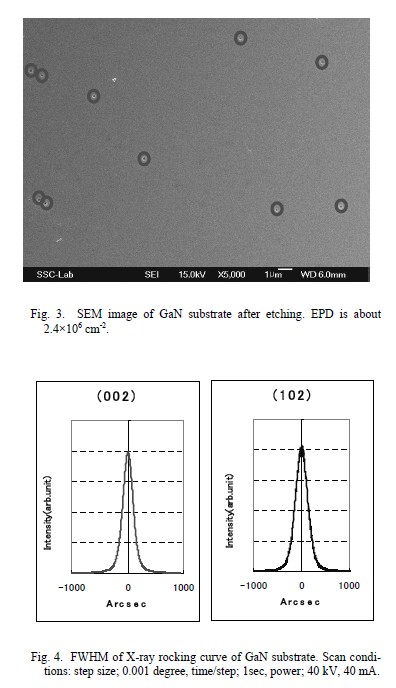
Figure 2 shows double crystal XRD profiles of the
GaN (002) and (102) plane in ω-scan. The full width at half maximum (FWHM) is
72 and 85 arcsec, respectively. Crystal quality of the GaN substrate was also
evaluated by etch pit density (EPD). After the etching the number of etch pits
was counted by SEM observation. The EPD is counted about 2.4×106 cm-2
(Fig. 3). Transmission electron microscopy (TEM) has been the general method to
measure the dislocation density, despite of the extensive and skillful sample
preparation process.12) However, in case of GaN films having low defect
densities such as below ~107cm-2, TEM method may be
uncertain and has difficulties observing the number of threading dislocations
due to the small measurement areas.11) Oshima et al. reported that the dislocation
density of Void-Assisted Separation (VAS) GaN was 5×106 cm-2
by EPD measurement.13) Motoki et al. reported that the measured
dislocation values were 5×10⁵, 2×10⁵ and 4×10⁴
cm-2 by EPD, TEM and cathodeluminescence measurements, respectively.14)
This result shows that there are some differences in measured dislocation
density by the measurement method. Considering the uncertainty of measured EPD
of about 2.4×106 cm-2, this result reveals that
conventional HVPE system could be used for the low dislocation density GaN
growth without ELO technologies.
Figure 4 shows the double crystal XRD profiles of
the 13 µm thin GaN template in ω-scan. The FWHM of (002) and (102) plane is 224
and 299 arcsec, respectively. These values are compatible with that of
metalorganic chemical vapor deposition (MOCVD) GaN films of 2 µm thick. Despite
rather thick GaN templates by HVPE compared to

MOCVD GaN, GaN templates could be used instead
of MOCVD GaN due to its rather low dislocation density of middle of 108
cm-2 of dislocation density (Fig. 5). The issues of rough surface of
HVPE GaN template so could be solved by precise process control. Figure 6 shows
the roughness of GaN template compared with MOCVD GaN measured by optical 3D
surface profiler. Although HVPE GaN template has about 2 times higher roughness
than that of MOCVD GaN, the optical microscope shows that the roughness of
homoepitaxial GaN on HVPE GaN could be used instead of MOCVD GaN.
4.
Summary
Free standing GaN thick films with low defect
density which is suitable for the high power blue laser diode manufacturing
were grown on sapphire by HVPE. Using the same HVPE growth technology, GaN
templates with moderate surface roughness and defect density (~5×10⁸
cm-2), which is suitable for high power LED manufacturing were grown
on sapphire by HVPE.
1) S. Nakamura and G. Fasol: The Blue Laser
diode (Springer Verlag,Berlin, 1997).
 2) H.
Amano, N. Sawaki, I. Akasaki and Y. Toyoda: Appl. Phys. Lett. 48(1986) 353.
2) H.
Amano, N. Sawaki, I. Akasaki and Y. Toyoda: Appl. Phys. Lett. 48(1986) 353.
3) S.
Nakamura: Jpn. J. Appl. Phys. 30 (1991)
L1705.
4) S.
Nakamura, M. Senoh, S. Nagahama, N. Iwasa, To. Yamada, T.Matsushita, H. Kiyoku,
Y. Sugimoto, T. Kozaki, H. Umemoto, M.Sano and K. Chocho: Jpn. J. Appl. Phys. 37 (1998) L627.
5) T.
Mukai and S. Nakamura: Jpn. J. Appl. Phys. 38 (1999) 5735.
6) A.
Usui, H. Sunakawa, A. Sakai and A. Yamaguchi: Jpn. J. Appl.Phys. 36 (1997) L899.
7) H.
Marchand, X. H. Wu, J. C. Ibbetson, P. T. Fini, P. Kozodoy, S.Keller, J. S.
Speck, S. P. DenBaars and U.K. Mishra: Appl. Phys. Lett.73 (1998) 747.
8) H.
Sone, S. Nambu, Y. Kawaguchi, M. Yamaguchi, H. Miyake, K.Hiramatsu, Y.
Iyechika, T. Maeda and N. Sawaki: Jpn. J. Appl. Phys.38 (1999) L356.
9) S.
S. Park, I. W. Park and S. H. Choh: Jpn. J. Appl. Phys. 39 (2000)L1141.
10)
M. K. Kelly, R. P. Vaudo, V. M. Phanse, L. Gögens, O. Ambacher and M. Stutzmann:
Jpn. J. Appl. Phys. 38 (1999)
L217.
11)
K. Lee and K. Auh: Jpn. J. Appl. Phys. 40
(2001) L13.
12)
L. T. Romano, B. S. Krusor and R. J. Molnar, Appl. Phys. Lett. 71(1997) 2283.
13)
Y. Oshima, T. Eri, M. Shibata, H. Sunakawa, K. Kobayashi, T. Ichihashi and A.
Usui: Jpn. J. Appl. Phys. 42 (2003)
L1.
14)
K. Motoki, T. Okahisa, S. Nakahata, N. Matsumoto, H. Kimura, K.Takemoto, K.
Uematsu, M. Ueno, Y. Kumagai, A. Koukitu and H.Seki: J. Cryst. Growth 237 (2002) 912.
No comments:
Post a Comment